Structure
To achieve the proposed objectives, this project is divided into 2 main parts:
Materials and Devices, organized in the following tasks:
1) Development of new multifunctional n and ptype MOS;
2) Nanoscale engineering of dielectric materials and composites;
3) High Throughput Materials characterization;
4) Thin film transistors and ICs;
5) Biosensors based on EIS and ISFETs;
6) Paper electronics;
7) Electrochromic field effect transistors;
8) Dissemination.
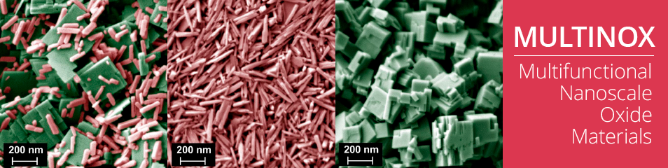
The MOS to be developed will be processed by PVD techniques like rf magnetron sputtering at RT, compatible with the use of low cost and flexible substrates, as a proof of concept and after that solution/suspension based techniques will also be used to turn viable the use of very low cost technologies as are the case of inkjet. These will facilitate a migration away from traditional “Si like” fab based batch processing to large area, which will offer a significant advantage in terms of reduced cost with increased throughput due to fewer manufacturing steps, especially for disposable devices/electronics.
The MOS to be developed will be processed by PVD techniques like rf magnetron sputtering at RT, compatible with the use of low cost and flexible substrates, as a proof of concept and after that solution/suspension based techniques will also be used to turn viable the use of very low cost technologies as are the case of inkjet. These will facilitate a migration away from traditional “Si like” fab based batch processing to large area, which will offer a significant advantage in terms of reduced cost with increased throughput due to fewer manufacturing steps, especially for disposable devices/electronics.
