Equipments and Resources
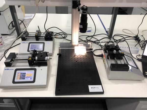
All microfluidic devices are tested here. Our current setup includes syringe pumps, a CMOS camera with an objective lens connected to a computer for image and video processing as well as a custom built LED lighting setup beneath the test platform.
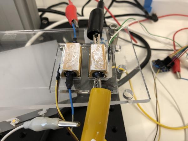
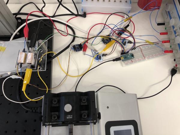
We are currently developing a heating system based on Joule effect through two different resistors. These are controlled an Arduino board and independent PT100 that will measure the resistors' temperature and, according each resistor setpoint, will allow current to flow through the it or not. Currently, we are aiming to perform PCR with two different temperatures at 95 ºC and 53 ºC.
The thin-film deposition area is an ISO 7 lab devoted to the preparation of thin films by physical and chemical vapor deposition techniques, as required to fabricate micro/nanoscale devices. The lab is equipped with a wide range of physical and chemical vapor deposition tools to fabricate a variety of thin film materials, such as metals, (transparent) conductors and semiconductors and insulators, with nm-thickness control. Most systems can accommodate up to 6” wafers.
This lab is equipped with all the required tools to achieve features sizes down to 1 µm (UV Hg lamp), 600 nm (UV laser diode) and 50-100 nm (nanoimprint) in layers composing micro/nanoscale devices. Wafers up to 6” diameter can be processed in spinners (resist deposition and development), hot plates, UV mask aligner, direct laser writer, substrate conformable nanoimprint lithography (SCIL, add-on to the UV mask aligner), wet etching benches and reactive ion etching tools. Available processes can make use of positive and negative tone resists as well as PDMS. There is also a LPCVD unit to fabricate polycrystalline Si thin films in substrate sizes up to 4”.